Clean Room Laboratory
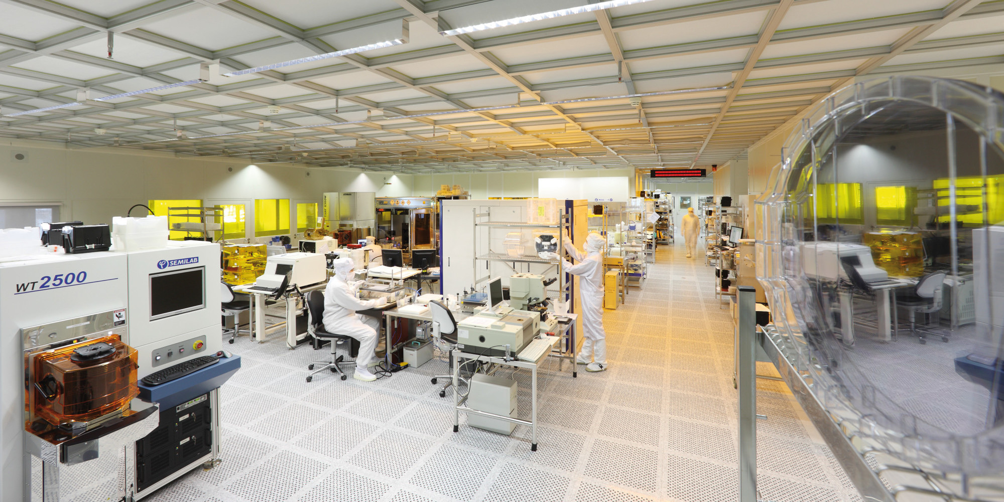
The Chair of Electron Devices maintains a cleanroom facility with a laboratory area of 600 square meters of class 10 and 400 square meters of class 1000. The modern equipment offers excellent conditions for the complex research tasks in the field of micro and nanoelectronics.
Together with the Fraunhofer IISB, a comprehensive processing technology is operated, which enables CMOS-compatible processing steps for the production of test structures and test devices in 150 millimeter silicon technology. Individual process steps are available for wafer sizes up to 300 millimeters. In addition, LEB operates a pilot line for the production of devices on silicon carbide substrates.
Within the work areas semiconductor and nanotechnology, semiconductor manufacturing equipment and methods as well as technology and device simulation, research is done which is complementary in the development, optimization and implementation of process steps in microelectronics manufacturing. The IISB is expanding its research spectrum to include crystal growing.
In all areas, there is close international cooperation with other research institutions and industry.